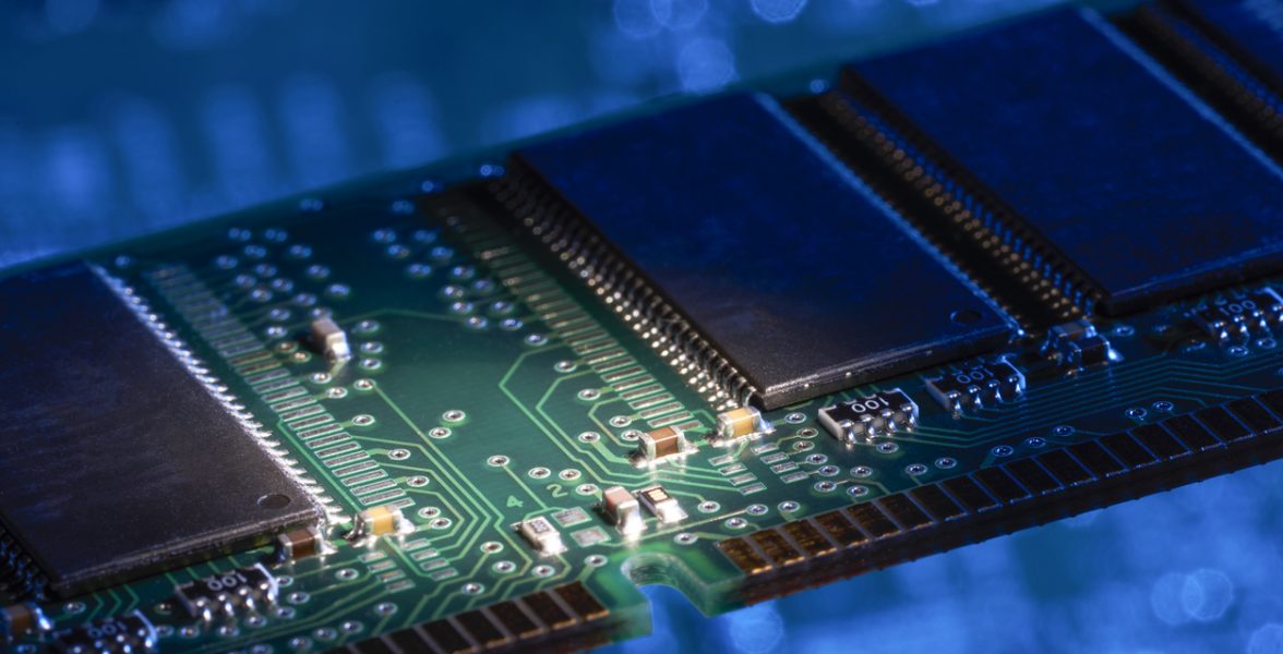
PCBリバースエンジニアリング(時にはPCB抽出やPCB切り取りとも呼ばれます)は、物理的なボードを使用してその部品をリバースエンジニアリングすることで、どのように作られたかについて学ぶことを目的としたプロセスです
PCBリバースエンジニアリングとは何ですか?
PCBリバースエンジニアリング(時にはPCB抽出またはPCB切断とも呼ばれます)は、物理的なボードを取り、その部品を逆エンジニアリングすることを意味します。これによって、そのボードがどのように作られたかについて学ぶことができます。これは、PCBの設計や構造を研究するためによく使われ、改善またはデバッグするために役立ちます。
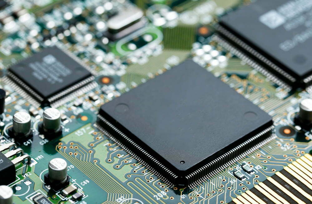
Our PCB reverse engineering services
Our PCB design and debugging engineers will guarantee to make 100% accurate schematic diagrams and perfect prototypes for you.
All Service of Reverse PCB
Support industries
Reverse engineering pros and cons
PCB prototyping boards are different types of PCBs designed for testing and evaluation. These prototypes can be used to evaluate the performance of your design prior to starting mass production or assembly. PCB Prototype Boards include:
how to reverse engineer a circuit board?
There are three main components of a circuit board: the substrate (mostly plastic), the circuit components, and the interconnects. The substrate contains all the holes and electrical connections for the circuit board and may have very little to do with the circuit. The circuit components are the components of the board that have a specific function, such as a microcontroller. Finally, the interconnects are the connections between every component on the board that allows the circuit to function. Once you know the components, it’s easy to reverse engineer a circuit board.
Step1: Take Pictures of the Circuit Board
This may seem basic, but it’s something that a lot of reverse engineers don’t do. First of all, it may seem unimportant, but it’s actually very important. If you don’t take pictures of the board, you won’t be able to reverse engineer it. All you’ll have is samples of the board, and then you’ll have to try to piece everything together yourself. Taking pictures of the board is essential for reverse engineering, so make sure you do it.
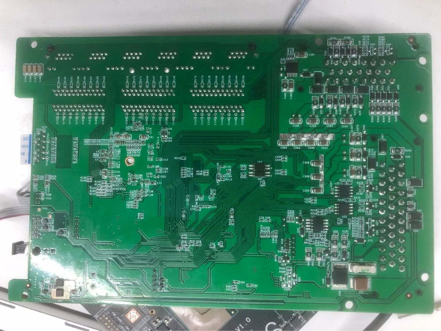
Step2: Trace Components
Next, trace the components on the board. This may seem like common sense, but a lot of reverse engineers don’t do it. By tracing components, you can figure out what components the board has, what their specifications are, and what their prices are. You can even use a multimeter to read the traces and determine what they do.

Step3: Construct PCB Layout
Reverse engineering a PCB involves creating a 3D layout of the board. This helps to visualize the electromagnetic field distribution and how different circuits behave. Additionally, it shows other aspects of the PCB that cannot be observed in a schematic, such as components, conductive elements, trace arrangement, and planes for each layer.
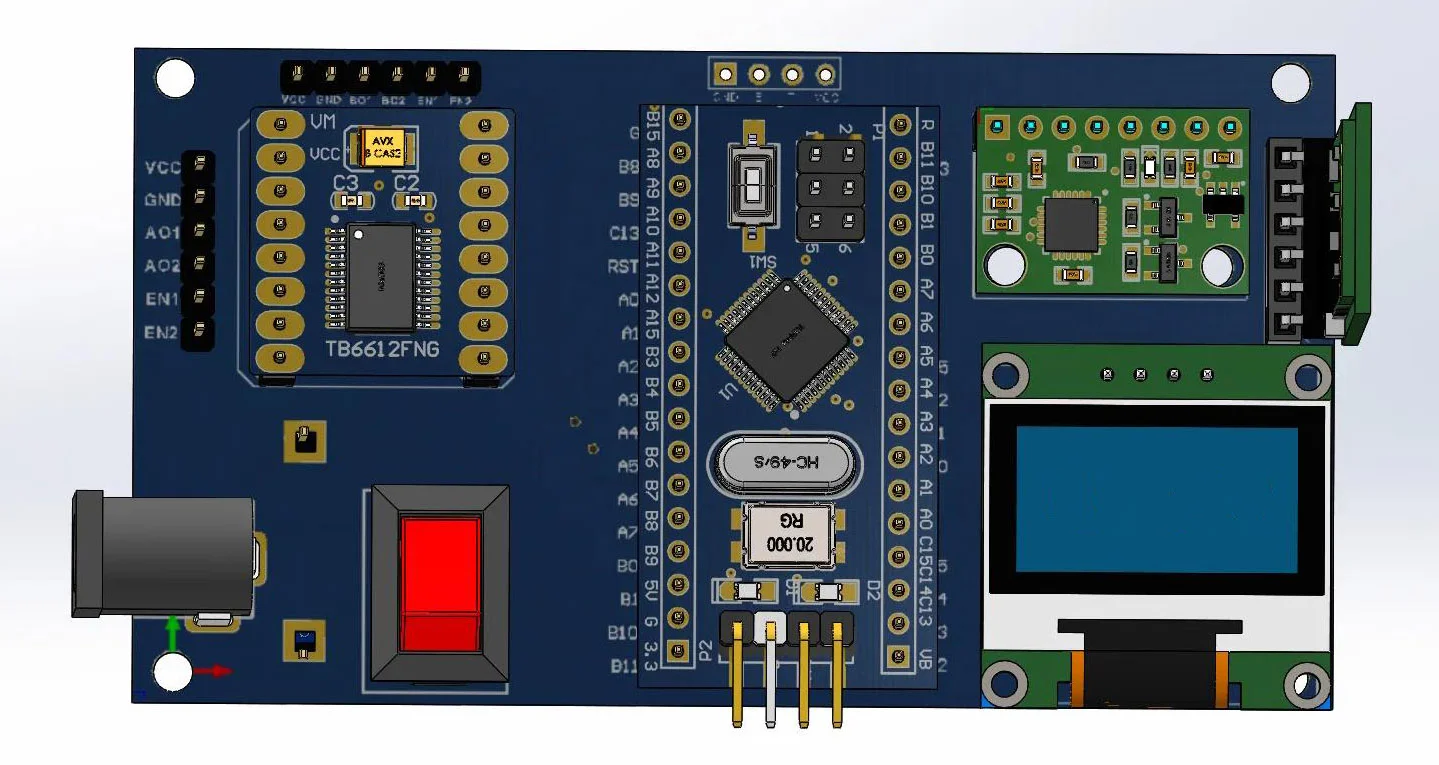
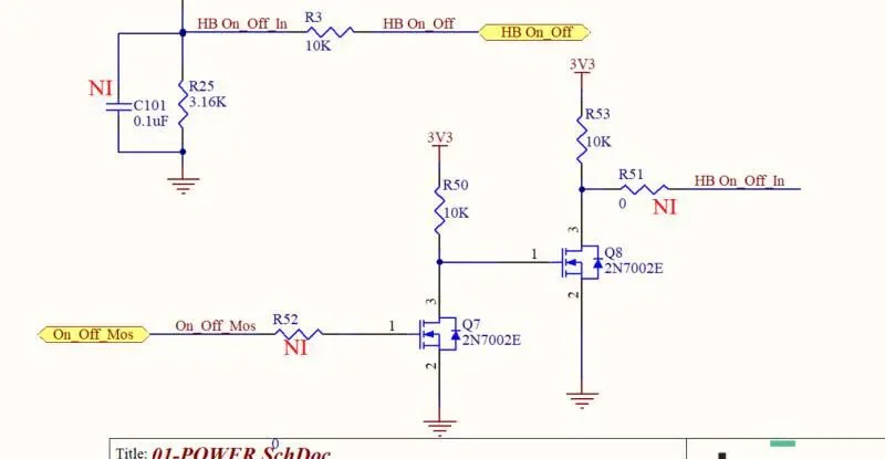
Step4: Create PCB Schematics
When you derive a PCB’s schematic diagram, you can see every circuit and all of the board’s components in two dimensions. This helps an engineer understand how different components connect and what their functionalities are. All of this information is crucial when repairing or reproducing a PCB.
Step5: Assemble the Circuit Board
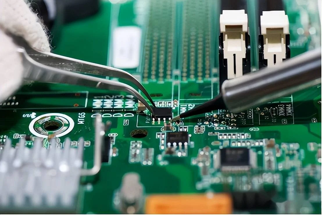
Now that you have a good idea of how the board is made, you can start reverse-engineering it. First, trace all of the components on the board and write down their specifications. Next, identify the board’s components, and their specifications. From there, assemble the board by putting the components on the circuit board.
PCB Reverse Engineering Cost
PCB Reverse Engineering costs are dependent on a variety of factors, such as complexity of the design, circuit characteristics, scope of the project, workload, etc. Unless the input data at the time of quotation is imperfect, or major engineering changes result in significantly longer delivery times, our quotations are fixed of. Here is a detailed breakdown of what costs you and how much it will cost you.


